The Technologies of the Photovoltaic
The production technologies of the photovoltaic cells are mainly divided into three groups:
| - |
Crystalline
silicium:
it can be monocrystalline or polycrystalline. |
| - |
Thin film: traditional amorphus,
multi junction systems (triple junction – CIS – CIGS),
the electrochemical cell of Graetzel. |
| - |
Gallium arsenide. |
 CRYSTALLINE
SILICIUM (c-Si) CRYSTALLINE
SILICIUM (c-Si)
At the moment the crystalline silicium is the most used from the
industrial point of view.
It is divided into POLYCRYSTALLINE (mc-Si) and MONOCRYSTALLINE
SILICIUM (Cz-Si).
The reasons of this widespread use are mainly the costs compared
to the efficiency per m² of the photovoltaic module and the
easiness of finding the silicium on the Earth. However, the refining
of the silicium itself is not so easy. It has to be pure at 99,9%,
fused into ingots and then cut into slices (wafers). The cells
in monocrystalline silicium can be also obtained through wafers
rejected by the microprocessors industry. These wafers are pickled
through simple acide attacks and then grown as photovoltaic cells.
However, this production technology “suffers” from
the optimization of the microchips production, which was able to
decrease the rejects thanks to the research.
The improvement curve of the crystalline silicium technology is
almost at the peak, as industrial efficiencies of 15-17% have been
reached (the silicium efficiency in the laboratory is of 25% but
it is difficult that it becomes a parameter applicable to industrial
solutions too). Therefore, the research is now moving from the
material to the production technologies of the cell, optimizing
the rejects (losses for the ingots cuts, new materials for doping,
new systems for the cell growing, testuring, recovery of active
area with new systems of fingher deposition, ext.). A new and interesting
technology is called “Spheral Solar”: it uses microspheres
of crystalline silicium to obtain flexible cells, without realising
and cutting slices from ingots, avoiding losses and expensive technologies
for the ingot and cell growing.
At the moment, thanks to several financing programmes of the various
European and Extraeuropean governments, the silicium ingots and
wafers market has had a great boom with a consequent increase of
costs and difficulty in the availability.
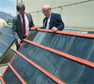
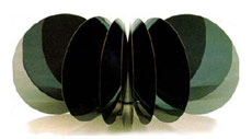 Wafers ready to become photovoltaic cells
 |
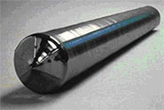 Ingot of crystalline silicium
 |
THIN FILM
TRADITIONAL AMORPHOUS SILICIUM (a-Si:H)
The technology of amorphous silicium was and continues
to be object of several investments in research and development.
It is surely the cheapest and simplest technology but it
is also the one granting the lowest efficiency: compared
to 16% of crystalline silicium, amorphous silicium reaches
6 – 8%. Moreover, only recently amorphous photovoltaic
modules have been realised with interesting warranties,
10 years versus 25 years of c-Si.
The creation process of the cell is very simple: more layers
of material are put on a rigid substrate (glass or metal)
through proper technologies (sputtering or evaporation),
two of these layers (the most external ones) become conduction
electrodes, while the inner layer becomes junction of the
photovoltaic cell. |
|
Composition of the a-Si:H cell
|
|
TANDEM & TRIPLE JUNCTION
a-Si:H TECHNOLOGY
This innovative technology derives from the traditional
a-Si:H and allows a bigger functioning efficiency, which
reaches, in some cases, 12% (triple junction). Further junctions
are added, treated in a different way, which have different
reactions to the light spectrum, increasing the functioning
band in the solar spectrum.
For example, a photovoltaic module realised with this type
of technology is able to produce 20% more of energy per year
compared to C-Si crystalline silicium because it has a better
reaction to the diffused solar radiation.
Unisolar Triple Junction technology (pictures on the right)
allows to realise flexible photovoltaic modules for various
uses and to stick the various cells on steel substrates (sheet
roofs) or roofs in other materials (PVC, ext.). Unisolar
is the only THIN FILM technology granting 20 years of warranty. |
|
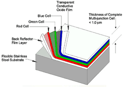
| Composition of Triple Junction cell and Unisolar PV module |
|
CADMIUM TELLURIUM/CADMIUM SULPHIDE TECHNOLOGY (CTS)
The solar cell CTS is composed by a p layer (CdTe) and by a n layer (CdS), which create a p-n heterojunction. The creation process is similar to the one of the Amorphous Silicium.
Unlike the a-Si:H technology, the cell CTS is able to reach bigger efficiencies: 8-10% for industrial products (15,8% reached in the laboratory).
One of the problems for the production in large scale of the CTS technology is the cadmium contained in the cell, which can become an environmental problem if it is not correctly recycled or used.
|
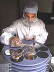
|
 Tests of PV cells with CTS technology
 |
COPPER INDIUM DISELENIDE AND COPPER INDIUM/GALLIUM DISELENIDE TECHNOLOGY (CIS and CIGS)
CIS, another thin film technology, is having a great success thanks to the recent research about copper/indium diselenide.
The results obtained show 13-15% of efficiency for cells tested in the laboratory, while adding gallium (CIGS) this value can even reach 18% for small cells. At the moment the value is about 10 11% for industrial cells.
It is expected that in the future CIS technology can give the same results of crystalline modules of the same size and power, but with much cheaper production costs.
GALLIUM ARSENIDE (GaAs) AND HIGH EFFICIENCY DEVICES
At the moment GaAs technology is the most interesting as regards efficiency, which is more than 25-30%, but the production of these cells is limited because of very high costs and shortage of raw material, which is mainly used in the industry of semiconductors at high speed of commutation and of optoelectronics (leds and phototransistors).
In fact GaAs technology is mainly used for space applications, where small weight and dimensions are very important. The results obtained with GaAs cells show a conversion efficiency of more than 30%.
In 1999 a project carried on by Spectrolab and National Renewable Energy Laboratory (NREL) reached an important record in the photovoltaic conversion, realising a solar cell with a conversion efficiency of 32,3%.
This triple junction cell has been manufactured using three layers of semiconductor materials, indium gallium phosphide, gallium arsenide and germanium (GaInP2/GaAs/Ge). In the near future further developments are expected, reaching 40% of efficiency.
|
|
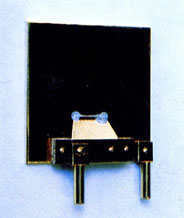 Cell with GaAs technology
 |
|
| |
» The
Technologies
|
|
 |
|
 |
|
